

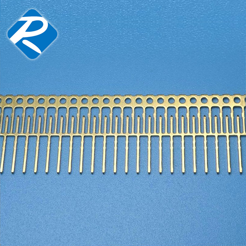
As core carrier components in the electronics industry, metal lead frames are widely used in semiconductor packaging fields. High‑quality stamping lead frames rely on mature Mold Processing technology, support diversified Custom Molds development, and become critical basic parts for modern Precision Manufacturing. The dimensional accuracy, surface flatness and material stability of lead frames directly affect the yield rate of chip packaging and the long‑term reliability of finished electronic products. Manufacturers pay strict attention to mold design, raw material selection and stamping tolerance control. This article analyzes this brass‑based stamping lead frame from product comparison, material science, application solutions and frequently‑asked questions.
Multiple types of lead frame production processes exist in the market, with obvious gaps in precision, cost and mass‑production stability. Chemical‑etched lead frames adopt chemical corrosion molding. They can realize complex graphics, yet suffer from high material loss and slow production speed, and are mainly suitable for small‑batch sample development. Simple‑stamping lead frames use ordinary single‑station molds. The mold structure is simple, but dimensional consistency is poor in mass production, burrs are easy to generate, and they cannot meet high‑end packaging requirements. In contrast, this continuous‑stamping metal lead frame is produced by high‑speed progressive die through professional Mold Processing. It supports personalized size adjustment via Custom Molds, perfectly matching the requirements of Precision Manufacturing. Compared with etching products, stamping process achieves higher production efficiency and lower unit cost for large‑volume orders. Compared with simple single‑station stamping, progressive‑die processing ensures tiny tolerance and uniform burr‑free surface. Its main limitation lies in high upfront investment for die development, more suitable for medium‑and‑large‑batch production. Customers can select processing solutions according to order quantity and drawing requirements.
Material performance lays the foundation for lead frame quality in Precision Manufacturing. High‑quality lead frames mostly adopt copper‑alloy base material, brass or phosphor‑copper strips. Copper‑alloy materials feature excellent electrical conductivity, good thermal conductivity and moderate hardness. During Mold Processing, the material shows outstanding ductility, not easy to crack during high‑speed punching. After stamping, surface plating treatment such as silver plating or nickel plating can be completed to improve weldability and anti‑oxidation performance. Reasonable Custom Molds design controls punching clearance accurately, effectively reducing burrs and material deformation. Many low‑cost products adopt impure copper‑mixed materials. Such raw materials have poor conductivity, unstable material hardness, prone to deformation and burr overflow in stamping. In subsequent semiconductor packaging, it may cause poor welding, virtual connection and other hidden troubles, bringing quality risks for downstream Precision Manufacturing. High‑grade raw materials plus standardized mold technology are the guarantee for qualified lead‑frame products.
This continuous‑stamping lead frame provides systematic application solutions for multiple industrial scenarios. First, semiconductor chip‑packaging solution: as core carrier for discrete components, diodes and triodes, cooperate with Mold Processing and Custom Molds to realize mass production of electronic components, supporting core links of Precision Manufacturing. Second, sensor‑component supporting solution: used for internal connection frames of miniature sensors, satisfy high‑precision size requirements of small‑size electronic parts. Third, optoelectronic‑device packaging solution: applied to LED and photoelectric component packaging, provide stable conductive channels for optoelectronic products. Fourth, non‑standard electronic‑component customization solution: develop exclusive Custom Molds according to customer drawings, realize non‑standard lead‑frame development for special‑specification components. Fifth, electronic‑factory spare‑part‑supply solution: provide standardized stamping lead‑frame raw materials for component factories, shorten internal Mold Processing cycle and reduce R&D investment. Purchasers shall confirm material specifications, plating requirements and dimensional tolerance before placing orders.
Below are common FAQs for lead‑frame procurement and usage in Precision Manufacturing.
Q1: What factors should be considered when selecting lead‑frame suppliers for Mold Processing and Custom Molds?
A: Focus on mold‑making capacity, stamping tolerance control, raw‑material grade, surface‑plating quality and mass‑production stability. Confirm whether they can provide targeted Custom Molds development to match your Precision Manufacturing demands.
Q2: What causes burrs on stamped lead frames?
A: Main reasons include unreasonable mold clearance, mold wear, poor raw‑material ductility. Optimize parameters in Mold Processing, maintain dies regularly, and select qualified copper‑alloy strip materials.
Q3: What influence does surface oxidation of lead frames bring to subsequent packaging?
A: Oxidation will cause poor welding performance, virtual soldering and reduced product yield. Lead‑frame products should be stored in dry environment, and plating treatment can enhance anti‑oxidation capacity.
Q4: Can etching and stamping processes be replaced arbitrarily?
A: Not recommended. Etching suits small‑batch complex patterns; stamping suits large‑batch regular‑structure products. Choose processing technology combined with batch quantity and drawing, and formulate corresponding Custom Molds.
Q5: Storage suggestions for stamping lead‑frame raw materials?
A: Keep sealed in dry‑constant‑humidity warehouse, avoid damp and corrosive gas. Prevent surface scratch during stacking, to ensure smooth follow‑up Precision Manufacturing processing.
Driven by the rapid development of electronic industry, higher standards are put forward for basic electronic components. High‑precision stamping lead frames rely on mature Mold Processing and flexible Custom Molds, providing reliable carrier support for Precision Manufacturing of semiconductors and electronic components. When purchasing, enterprises should attach importance to raw‑material quality and mold‑making level instead of only pursuing low unit price. Scientific storage and use can effectively improve downstream packaging yield and reduce production loss.
