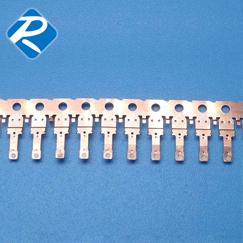
Semiconductor and electronic‑component industries are developing toward miniaturization and high‑density packaging. As indispensable basic conductive carriers, metal stamping lead frames are deeply connected with Mold Processing, Custom Molds and the whole chain of Precision Manufacturing. Mold‑design rationality, stamping‑process control and material performance directly determine product qualification rate. This article makes comprehensive interpretation from product comparison, material science popularization, multi‑scene application schemes and frequently‑asked questions.
Different lead‑frame forming technologies have respective advantages and limitations, rational comparison helps enterprises make scientific selection.
- Chemical‑etching lead frame: realize complex and fine patterns without expensive stamping dies. High material consumption, slow production speed, high unit price, suitable for small‑batch prototype verification, not fit for large‑scale Precision Manufacturing.
- Single‑station simple‑stamping lead frame: low die‑making cost, simple structure. Poor dimensional consistency for large‑batch production, many burr defects. Not suitable for high‑precision chip‑packaging scenarios, and cannot support complex‑structure Custom Molds.
- High‑speed progressive‑die stamping lead frame (this product): mainstream high‑volume product for electronic industry. Mature Mold Processing technology adopts progressive die structure. It supports personalized development via Custom Molds, features high‑speed continuous production, stable dimensional tolerance, few burrs, high efficiency, perfectly matching mass‑production demands of Precision Manufacturing. Its disadvantage is high initial die‑development cost, economical only under medium‑and‑large‑batch orders.
Raw‑material quality and die‑making craft are core factors of high‑performance lead frames for Precision Manufacturing. Qualified lead frames mostly adopt copper‑alloy strip such as brass and phosphor copper. Copper‑alloy owns excellent electric‑thermal conductivity and good ductility. In the process of Mold Processing, materials can complete fine punching without cracking. Through precise clearance design of Custom Molds, the stamping process effectively controls deformation and burr problems. Subsequent surface nickel‑plating or silver‑plating treatment improves weldability and anti‑tarnish performance. Many low‑cost products adopt inferior mixed‑copper materials. With unstable hardness and poor conductivity, they are easy to deform during stamping. Such defective products will trigger virtual welding and circuit failure in downstream packaging, bringing huge hidden danger to Precision Manufacturing. Premium raw materials and sophisticated mold‑making are the core guarantee of high‑quality lead frames.
High‑speed stamped lead frames provide complete supporting solutions for multiple electronic‑manufacturing fields.
- Discrete‑device‑packaging solution: serve as conductive carrier for diodes, triodes and MOS tubes. Realize mass production through stable Mold Processing, and realize special‑size iteration by Custom Molds, supporting large‑scale Precision Manufacturing.
- LED‑optoelectronic‑component solution: applied to LED lamp‑bead internal bracket, satisfy miniaturization and high‑density production requirements of optoelectronic products.
- Micro‑sensor‑manufacturing solution: used for internal connecting frame of miniature sensors, adapt to fine‑pin and small‑size product characteristics.
- Sample‑customization and small‑batch‑verification solution: combine etching and stamping technology. Develop targeted Custom Molds according to customer drawings, meet the demand of new‑product R&D.
- Component‑factory raw‑material‑supply solution: supply roll‑type continuous‑stamping lead‑frame materials for electronic‑packaging factories, save internal Mold Processing investment and shorten product‑launch cycle.
Summarize frequently‑asked questions in actual production application of lead‑frames for Precision Manufacturing.
Q1: How to choose between etching and stamping when launching new projects for Mold Processing and Custom Molds?
A: Small‑batch prototype adopts etching process; after project confirmation and mass‑production preparation, invest in progressive‑die Custom Molds, switch to stamping process to reduce unit cost for formal Precision Manufacturing.
Q2: What causes lead‑frame deformation after stamping?
A: Reasons include unreasonable mold clearance, unstable material hardness, improper material‑strip tension during high‑speed stamping. Optimize die parameters in Mold Processing and select qualified copper‑alloy strip.
Q3: Why is surface plating treatment required for lead frames?
A: Plating improves solderability and anti‑oxidation performance. Without plating, copper‑alloy surface is easy to oxidize, resulting in poor welding in subsequent packaging and reducing finished‑product yield.
Q4: Can the existing Custom Molds be modified to realize size adjustment?
A: Partial dimension adjustment can be realized by modifying molds, but too‑large‑range change needs newly‑developed molds. It is suggested to communicate with mold‑manufacturing engineer in early stage of Mold Processing.
Q5: What risks will improper storage bring to lead‑frame products?
A: Damp environment causes oxidation; friction and scratch damage plating layer. Sealed dry‑warehouse storage is required to guarantee smooth follow‑up Precision Manufacturing.
Benefiting from the vigorous growth of semiconductor and consumer‑electronics industries, the market demand for precision stamping lead‑frames keeps expanding. Relying on mature Mold Processing and flexible Custom Molds, lead‑frame products provide solid basic‑component support for Precision Manufacturing. When selecting suppliers, enterprises should comprehensively assess raw‑material grade, mold‑making strength and process‑control capacity, instead of focusing only on quotation. Reasonable application and storage can effectively lower downstream production risks and improve overall production‑chain benefit.